Category: video games

PS5 Pro Specs Breakdown: PSSR, GPU Architecture & Frame Rates

PS5 Pro Specs Breakdown: PSSR, GPU Architecture & Frame Rates

PS5 Pro Specs Breakdown: PSSR, GPU Upgrades, and Frame Rates Explained

Editor’s Note: When Sony launched the PlayStation 5 Pro, it marked a fundamental shift in how mid-generation console refreshes are engineered. Rather than relying solely on brute-force silicon growth or pushing native pixel counts to unsustainable levels, the PS5 Pro leans into machine-learning upscaling, hybrid ray-tracing architectures, and offloaded system memory. Here is a complete technical breakdown of how the PS5 Pro’s 67% GPU expansion, PSSR AI pipeline, and boosted memory subsystem translate to real-world gaming performance—and how this hardware lays the groundwork for Sony’s long-term console strategy.

1. Executive Overview: The Mid-Gen Shift

During the PS4 Pro era, the objective of mid-generation hardware was straightforward: bridge the gap from 1080p HDTVs to early 4K displays. However, native 4K rendering at high frame rates rapidly became an expensive bottleneck for modern rendering pipelines. High-geometry meshes, complex volumetric lighting, and real-time ray tracing demand immense compute cycles that traditional brute-force resolution scaling cannot sustain within a standard living room power envelope.

The PS5 Pro alters this philosophy. Instead of sacrificing frame rates to hit arbitrary internal render targets, the console targets a stable 4K at 60 FPS baseline across demanding titles.

Base PS5 Paradigm: Fidelity Mode (30 FPS @ Native 4K) VS. Performance Mode (60 FPS @ Lower Res)
PS5 Pro Paradigm: PS5 Pro Enhanced (60 FPS @ 4K Reconstruction + Ray Tracing)

By collapsing the forced choice between 30 FPS “Fidelity” and 60 FPS “Performance” modes, the console focuses its hardware upgrades on three main pillars:

  1. An expanded GPU die with accelerated ray-tracing blocks.
  2. Dedicated hardware AI upscaling via PlayStation Spectral Super Resolution (PSSR).
  3. A refined memory topology that offloads background tasks to maintain high bandwidth availability.

Beyond the core silicon, the console integrates a standard 2TB NVMe SSD to accommodate ballooning game install sizes, supports Wi-Fi 7 (802.11be) for reduced network jitter, and increases peak power delivery to 390W while maintaining a slim form factor similar to the base model.

2. GPU Architecture & The Ray Tracing Engine

At the heart of the PS5 Pro’s custom System-on-Chip (SoC)—codenamed “Viola”—lies a substantial graphics upgrade manufactured on a 4nm TSMC process node.

Base PS5 GPU: 36 Compute Units (RDNA 2) ➜ 10.28 TFLOPS
PS5 Pro GPU: 60 Compute Units (RDNA 3/4 Hybrid) ➜ 16.7 TFLOPS (Base) / ~33.5 TFLOPS (Dual-Issue)

Compute Unit Expansion & Dual-Issue FP32

The base PS5 utilizes 36 RDNA 2 Compute Units (CUs) clocked up to 2.23 GHz, yielding 10.28 TFLOPS of single-precision (FP32) performance. The PS5 Pro expands this configuration to 60 active Compute Units (3,840 shading units) built on a hybrid AMD graphics architecture:

  • Rasterization Throughput: The 67% increase in compute units, combined with 240 Texture Mapping Units (TMUs) and 64 ROPs, delivers approximately 45% faster raw rasterized rendering.
  • Dual-Issue FP32 Execution: Utilizing RDNA 3 instruction sets, each execution unit can execute two mathematical operations per clock cycle. This pushes mathematical peak compute from a base 16.7 TFLOPS up to ~33.5 TFLOPS when dual-issue instructions are fully saturated by game engines.

Hybrid RDNA 4 Ray Tracing Blocks

While rasterization gains are significant, the biggest architectural jump occurs in real-time ray tracing. The PS5 Pro integrates specialized ray-tracing hardware blocks derived from AMD’s RDNA 4 architecture.

Unlike base RDNA 2 hardware, which handled Bounding Volume Hierarchy (BVH) ray traversal largely in software on standard compute shaders, the PS5 Pro features dedicated 2nd-generation ray-tracing accelerometers:

  • Ray-Triangle Intersection Hardware: Multiplies ray-tracing traversal speed by 2x to 4x compared to the base PS5.
  • BVH8 Traversal Support: The hardware can evaluate 8-node BVH trees per cycle (up from 4-node structures), significantly reducing the CPU overhead and execution stalls traditionally associated with complex reflections, ambient occlusion, and dynamic global illumination.

3. PSSR Deep Dive: Machine Learning Upscaling

Brute-force rendering at native 3840×2160 requires an extraordinary amount of fill-rate and memory bandwidth. To solve this, Sony introduced PlayStation Spectral Super Resolution (PSSR), a proprietary, hardware-accelerated temporal upscaling pipeline.

Lower Render Resolution (e.g., 1200p - 1440p)
│
▼
Temporal Motion Vectors + Depth Buffers + Frame History
│
▼
PS5 Pro Custom NPU (Tensor Matrix Operations)
│
▼
Sharp, Reconstructed 4K Output (60 FPS)

How PSSR Works Under the Hood

Unlike software-based spatial upscalers, PSSR utilizes a trained deep-learning neural network running directly on dedicated Neural Processing Unit (NPU) hardware embedded within the Viola SoC.

  1. Temporal Data Ingestion: PSSR takes a lower-resolution render target (typically between 1080p and 1440p), current frame motion vectors, depth buffers, and historical frame data.
  2. Convolutional Neural Inference: The NPU evaluates sub-pixel jitter and motion fields to reconstruct fine details—such as thin power lines, foliage, chain-link fences, and specular highlights—that traditional spatial upscaling loses or blurs.
  3. Artifact Mitigation: Because PSSR operates at the hardware level with temporal feedback loops, it minimizes the visual “flicker,” edge moiré, and temporal instability common in spatial post-processing filters.

PSSR vs. DLSS and FSR

While AMD’s FSR 2 and FSR 3 rely on hand-tuned algorithms running on general-purpose GPU shaders, PSSR delegates work to dedicated tensor cores, similar to NVIDIA’s Deep Learning Super Sampling (DLSS). This frees up valuable GPU compute units to concentrate entirely on shading, geometry, and lighting effects rather than image reconstruction.

🔗 Looking Ahead: PSSR represents Sony’s first step into machine-learning pipelines. For an in-depth look at how this technology evolves into PSSR 2.0 on next-gen hardware, read our complete PS6 ‘Orion’ hardware analysis

.

4. Memory System & Subsystem Architecture

A common bottleneck in high-performance graphics architecture is memory bus contention—the clash between the CPU, GPU, and operating system when requesting access to the same system RAM pool.

Base PS5 Memory Allocation: 16GB GDDR6 Shared (12.5GB Games / 3.5GB OS)
PS5 Pro Memory Allocation: 16GB GDDR6 (13.7GB Games) + 2GB DDR5 (Dedicated OS)

GDDR6 Bandwidth Elevation

The PS5 Pro maintains a 256-bit memory bus but upgrades its GDDR6 memory modules from 14 Gbps to 18 Gbps. This elevates total system memory bandwidth from 448 GB/s to 576 GB/s—a clean 28% increase in raw data throughput.

The 2GB DDR5 OS Offload

To maximize available VRAM for game developers, Sony made a critical physical addition to the motherboard: a secondary 2GB DDR5 memory chip.

  • Operating System Isolation: In the base PS5, the operating system reserved roughly 3.5GB of the primary GDDR6 pool. On the PS5 Pro, background OS functions, system apps, and video capture buffers are moved to the secondary DDR5 module.
  • Expanded VRAM Allocation: Offloading background tasks frees up an additional ~1.2GB of fast GDDR6 VRAM specifically for game developers, expanding the usable VRAM pool for games to approximately 13.7GB. This extra space is crucial for storing high-resolution PSSR frame buffers and ray-tracing acceleration structures.

CPU High-Frequency Mode

The central processor remains an 8-core, 16-thread AMD Zen 2 CPU, but includes a software-selectable High CPU Frequency Mode:

  • Base CPU Clock: 3.5 GHz (Fixed).
  • High Frequency Mode: Pushes CPU clocks by 10% to 3.85 GHz.
  • Operating in High Frequency Mode reallocates roughly 1% to 2% of GPU power to the CPU, providing developer flexibility in CPU-bound scenarios (such as complex crowd AI or high-draw-call simulation logic).

Technical Specifications Comparison

Hardware FeatureBase PlayStation 5PlayStation 5 ProArchitectural Uplift
Process NodeTSMC 7nm / 6nmTSMC 4nm (Viola SoC)Higher transistor density & efficiency
GPU Compute Units36 CUs (RDNA 2)60 CUs (RDNA 3/4 Hybrid)+67% Compute Units
Raw Compute (FP32)10.28 TFLOPS16.7 TFLOPS (Base) / ~33.5 TFLOPS (Dual-Issue)+45% Rasterization Speed
Ray Tracing EngineRDNA 2 Hardware RTRDNA 4 Hardware RT Blocks2x – 4x Ray Traversal Throughput
AI ReconstructionSoftware FSR / SpatialHardware PSSR (Dedicated NPU)Machine-Learning Temporal Upscaling
Primary System RAM16GB GDDR6 @ 448 GB/s16GB GDDR6 @ 576 GB/s+28% Bandwidth Boost
Secondary RAMNone2GB DDR5 (Dedicated OS Pool)+1.2GB VRAM Free for Games
CPU Architecture8x Zen 2 @ 3.5 GHz8x Zen 2 @ up to 3.85 GHz+10% High-Frequency Mode
Internal Storage825 GB NVMe SSD2 TB NVMe SSD+142% Baseline Capacity
Wireless NetworkWi-Fi 6 (802.11ax)Wi-Fi 7 (802.11be)Lower latency wireless streaming

5. Real-World Frame Rates & “PS5 Pro Enhanced” Performance

All of these hardware enhancements converge under Sony’s “PS5 Pro Enhanced” software guidelines. To earn the label, developers must utilize the console’s added power to deliver clear visual improvements over standard PS5 profiles.

Key Performance Targets in Modern Engines

  1. 60 FPS Ray-Traced Fidelity: Games that previously forced players into 30 FPS mode to enjoy ray-traced reflections—such as Marvel’s Spider-Man 2, Ratchet & Clank: Rift Apart, and The Last of Us Part II Remastered—run at 60 FPS while retaining high-fidelity visual settings.
  2. PSSR Image Stabilization: Titles featuring dynamic resolution scaling no longer drop to soft 1080p presentation windows during intense alpha-effect scenes. PSSR reconstructs dynamic buffers to maintain a sharp 4K image on high-refresh-rate displays.
  3. PS4 Game Boost: System-level post-processing and frequency stabilization apply directly to legacy PlayStation 4 software, stabilizing unlocked frame rates and smoothing variable resolution presentation without requiring explicit developer patches.

By combining an expanded RDNA 3/4 hybrid GPU, dedicated DDR5 OS caching, and machine-learning frame reconstruction, the PS5 Pro delivers a refined, high-frame-rate console experience—and sets the technical baseline for the future of PlayStation hardware.
PS6 Specs & Release Date Leak: Orion SoC, GDDR7 & Cost Analysis

PS6 Specs & Release Date Leak: Orion SoC, GDDR7 & Cost Analysis

PS6 Hardware Analysis: Inside Codenamed ‘Orion’, GDDR7 Memory Architecture, and the $960 Silicon Cost

Executive Summary: Sony’s unannounced PlayStation 6 is shaping up to be one of the most technologically ambitious—and economically complex—console launches in modern gaming history. Leaked AMD engineering documents describe a 3nm system-on-chip codenamed “Orion” built around Zen 6 CPU cores and RDNA 5 graphics. However, a transition to high-speed GDDR7 memory and a global DRAM supply crunch driven by AI infrastructure demand have inflated component costs, driving the estimated Bill of Materials (BOM) to nearly $960 and forcing Sony to evaluate a delayed release window of 2028 or 2029.

1. What Is PS6 “Orion”? Architectural Deep Dive

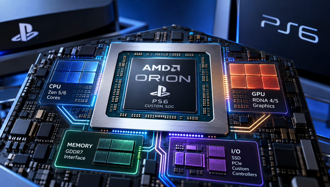
While Sony has not formally announced the PlayStation 6, hardware leaks from reputable semiconductor channels point to an AMD semi-custom system-on-chip (SoC) codenamed Orion. Continuing a partnership that began with the PS4 in 2013, AMD is designing the silicon, which combines CPU and GPU blocks on a single monolithic die.

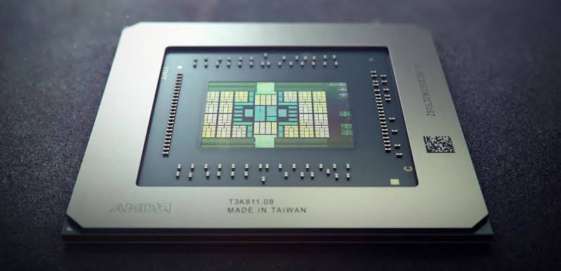
AMD semi-custom silicon architecture powering next-gen console hardware. Source: TechSpot

CPU & GPU Architecture

According to hardware documentation corroborated by tech publications TechSpot and TweakTown, Orion is targeted for TSMC’s 3nm process node with a die area of approximately 280mm² and a Thermal Design Power (TDP) capped near 160W (roughly 60W higher than the launch PS5):

  • CPU Microarchitecture: The central processor leverages AMD’s Zen 6 architecture, featuring 7 to 8 high-efficiency Zen 6c cores alongside dedicated low-power (LP) cores running at up to 3.0 GHz to handle operating system and background tasks seamlessly.
  • GPU & Ray Tracing Engine: Graphics are powered by RDNA 5 with 54 physical Compute Units (CUs), 52 of which are active (two disabled for manufacturing yield protection). Clocks run between 2.6 GHz and 3.0 GHz, supported by 10MB of L2 cache, delivering an estimated 34 to 40 TFLOPS of raw compute throughput. Ray tracing performance is rumored to achieve a 6x to 12x leap over baseline PS5 hardware.

2. GDDR7 vs. GDDR6: The Memory Architecture Breakdown

The shift from the PlayStation 5’s GDDR6 memory to GDDR7 represents one of the most substantial architectural leaps in next-generation console hardware.

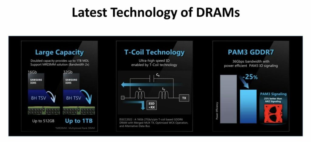
GDDR7 utilizes PAM3 signaling to deliver higher bandwidth with improved power efficiency. Source: Wccftech

PAM3 Encoding vs. Legacy NRZ Signaling

The primary technical breakthrough of GDDR7 lies in its physical layer signaling protocol:

  • GDDR6 (NRZ / PAM2): Uses Non-Return-to-Zero (NRZ) signaling, transmitting 1 bit of data per cycle using two voltage levels (0 or 1). As signal frequencies scale beyond 20–24 Gbps, noise and signal attenuation on standard printed circuit boards (PCBs) degrade reliability significantly.
  • GDDR7 (PAM3): Adopts Pulse Amplitude Modulation 3-level (PAM3) encoding. By using three distinct voltage levels (-1, 0, +1), PAM3 transmits 3 bits of data over 2 clock cycles (1.5 bits per cycle). This achieves a 50% increase in data transmission efficiency over NRZ at the same operating clock frequency.
GDDR6 (NRZ / 2-Level): [ High ] -> 1 [ Low ] -> 0 (1 bit / cycle)
GDDR7 (PAM3 / 3-Level): [ +1 ] / [ 0 ] / [ -1 ] (1.5 bits / cycle)

Bandwidth, Power Efficiency, and Bus Width

Because PAM3 reduces signal attenuation at high clock frequencies, GDDR7 memory modules can achieve speeds of 32 Gbps to 36 Gbps per pin, compared to GDDR6’s practical ceiling of 20–24 Gbps:

  1. Massive Bandwidth Increase: On a rumored 160-bit memory bus running at 32 Gbps, the PS6 would achieve approximately 640 GB/s of bandwidth—a 43% boost over the PS5’s 448 GB/s (and significantly higher than standard desktop GPU configurations).
  2. Power Efficiency: PAM3 signaling lowers the operating voltage and energy consumption per bit transmitted by roughly 20% to 25% compared to high-frequency GDDR6, keeping thermal output manageable within a console form factor.

Why GDDR7 Is Critical for Next-Gen Ray Tracing & AI Upscaling

Next-gen visual pipelines depend heavily on rapid memory access, far beyond what CPU and GPU compute cycles alone provide:

  • Complex Ray Tracing BVH Traversal: Real-time ray tracing requires continuous queries against Bounding Volume Hierarchy (BVH) structures stored in system RAM. GDDR7’s ultra-low latency and ~640 GB/s bandwidth prevent the GPU execution units from stalling during dense ray-triangle intersection checks.
  • Neural Upscaling (PSSR 2.0): Machine learning models (such as PlayStation Spectral Super Resolution) rely on high-throughput tensor operations that pull multiple high-resolution frame buffers, motion vectors, and temporal data arrays simultaneously. GDDR7 ensures the NPU hardware receives data streams without creating memory bottlenecks.

Memory Architecture & PSSR 2.0

The platform transitions from GDDR6 to high-speed GDDR7 memory, configured between 30GB and 40GB on a 160-bit bus running at 32Gbps. This yields approximately 640 GB/s of bandwidth—a ~43% increase over the PS5’s 448 GB/s. Dedicated neural processing units (NPU) will drive an expanded AI upscaling pipeline, provisionally designated PSSR 2.0 (PlayStation Spectral Super Resolution).

Hardware Comparison: PlayStation 5 vs. Rumored PS6 “Orion”

SpecificationPlayStation 5 (2020)PS6 “Orion” (Rumored / Unconfirmed)
Manufacturing ProcessTSMC 7nmTSMC 3nm
CPU Architecture8x Zen 2 cores @ 3.5 GHz7-8x Zen 6c + LP cores @ up to 3.0 GHz
GPU ArchitectureRDNA 2RDNA 5
Compute Units (CUs)36 CUs52 active CUs (54 physical)
Raw Compute10.28 TFLOPS34 – 40 TFLOPS
Memory System16GB GDDR6 (NRZ)30GB – 40GB GDDR7 (PAM3)
Memory Bandwidth448 GB/s~640 GB/s
Thermal Target (TDP)~100W – 115W~160W

3. The $960 Component Cost & Semiconductor Economics

The defining challenge for the next console generation is not raw silicon engineering, but macroeconomics in the memory market.

Industry analyst David Gibson (MST Financial) and Sony CEO Hiroki Totoki have both noted that global demand for high-bandwidth memory (HBM) and enterprise DRAM in AI data centers is straining consumer semiconductor supply chains. Speaking to investors, Totoki acknowledged that memory pricing is expected to remain significantly elevated through fiscal year 2027.

March 2026 (Initial BOM Estimate): ~$760
│
▼ +~$200 Memory & Silicon Price Inflation
June 2026 (Revised BOM Estimate): ~$960

Prominent hardware leaker Kepler_L2 initially estimated the PS6 Bill of Materials (BOM)—the direct cost of individual components prior to assembly, shipping, software licensing, and retailer margins—at approximately $760 in March 2026. By late June 2026, driven by spiking GDDR7 and wafer costs, Kepler_L2 revised that figure upward by $200 to ~$960.

4. Timeline Realignment: Why 2028 or 2029 Is Now the Likely Window

The shifting component landscape has directly altered Sony’s internal release target timeline over the past 12 months:

Early 2026 Leaks: Target Late 2027
│
├─ Bloomberg Report: RAM Shortage Forces Evaluation
├─ Sony CEO Statement: No Fixed Launch Date or Price
│
Current Industry Consensus: 2028 – 2029 Release Window
  • Early Projections: Early supply chain indications pointed to a late-2027 production ramp and holiday launch window.
  • Mid-Term Corrections: As memory cost pressures intensified, reporting from Bloomberg indicated Sony was evaluating a push into 2028 or 2029.
  • Official Stance: Sony leadership maintains that no release date or pricing structure has been finalized. Sliding the release date back allows memory fab capacity to normalize and reduces the risk of launching a console priced out of reach for core consumers.

5. Companion Strategy: “Project Canis” Handheld

To complement its flagship home console, leaks point to a standalone handheld device codenamed Project Canis. Unlike the PlayStation Portal (which relies exclusively on remote streaming), Canis is designed to run PlayStation games natively.

  • Architecture: Scaled-down Zen 6c CPU (4x Zen 6c + 2x Zen 6 LP cores) paired with an RDNA 5 GPU and 16GB to 24GB of LPDDR5X memory.
  • Performance Target: In docked mode, Canis is rumored to achieve 55%–75% of the baseline PS5’s rasterization performance and up to 2.6x its ray tracing output on a 1080p (60Hz/120Hz) display.
  • Software Ecosystem: The device is expected to leverage a native firmware “Low Power Mode” recently integrated into the PS5 operating system, enabling full backward compatibility with native PS4 and PS5 titles.

Fact Check & Summary Breakdown

QuestionStatusDetails
Has Sony officially announced PS6?❌ UnconfirmedSony has not formally named, displayed, or scheduled the console.
What is the reported codename?🔍 OrionLeaked AMD engineering documents identify the semi-custom SoC as “Orion.”
What is the current release window?📅 2028 – 2029Pushed back from earlier 2027 targets due to DRAM memory supply constraints.
How much will it cost?💰 TBD (BOM ~$960)Component cost leaks point to ~$960; retail strategy will balance subsidy vs. consumer demand.
Will it support backward compatibility?🔄 Likely YesArchitecture continuity (AMD x86-64 + Zen/RDNA) strongly supports backward compatibility with PS5 and PS4 libraries.

7. Frequently Asked Questions (FAQ)

Has Sony officially announced the PlayStation 6?

No. Sony has not officially announced, named, or scheduled a release date for the PlayStation 6. All specifications, internal codenames (“Orion”), and pricing figures stem from semiconductor supply chain leaks, analyst reports, and AMD engineering roadmaps.

What is the codename “Orion”?

“Orion” is reported to be the internal codename for the custom System-on-Chip (SoC) being developed by AMD for Sony’s next console, continuing the lineage of PS4’s “Liverpool” and PS5’s “Oberon.”

Why is the release date expected to be pushed to 2028 or 2029?

While earlier leaks targeted late 2027, an unprecedented global shortage of DRAM and GDDR memory—driven by heavy AI data center demand—has inflated component manufacturing costs. Pushing the console’s launch to 2028 or 2029 gives memory fabrication plants time to normalize supply and lower production costs.

How much will the PS6 cost at retail?

While the estimated Bill of Materials (BOM) has reached ~$960 according to leaker Kepler_L2, retail pricing has not been set. Analysts at Newzoo anticipate Sony will attempt to keep the final consumer price under $999 by subsidizing initial hardware units and recouping costs through digital game sales and PlayStation Plus subscriptions.

Will the PS6 be backward compatible with PS5 and PS4 games?

Yes. Because the PS6 uses AMD’s x86-64 CPU architecture and RDNA graphics architecture, native backward compatibility with existing PS5 and PS4 software libraries is an architectural certainty.

What is “Project Canis”?

Project Canis is the rumored internal codename for a dedicated PlayStation handheld device. Powered by AMD Zen 6c and RDNA 5 silicon, it is designed to run native PS4 and PS5 games on a 1080p portable screen rather than relying on cloud or remote play streaming.

Related Article

PS5 Pro Specs Breakdown: PSSR, GPU Architecture & Frame Rates